Showing posts with label Circuit. Show all posts

Monday, May 14, 2007

Driving Multiple VGA Monitors

At times, driving more than one monitor from a single PC video port is practical or necessary. Software demonstrations or other kinds of group demonstrations are examples of one type of occasion. Side-by-side comparisons of different brands of monitors are another. Also, certain artistic displays work best when more than one monitor displays an image.

Multiple monitor drivers that drive from two to sixteen monitors simultaneously are currently available. These devices start at about #300 and go up in price depending on the number of monitors the device can drive. However, the simple circuit I describe here is an alternative that addresses these problems at a much lower cost. I built the "core" of this circuit with three low-cost transistor chip arrays and a handful of resistors. Moreover, you can duplicate the core ad infinitum to drive as many monitors as demanded by the task at hand.

THE CIRCUIT

Figure 1 shows my multiple-monitor driver. This simple device implements any number of parallel emitter-follower amplifiers, which serve three essential purposes. The first is to provide a properly terminated load to the video card in the computer. Second, these amplifiers serve as isolation amplifiers between the PC video card and the multiple monitors being driven from the video source. The third purpose of these amplifiers is to provide drive current to the inputs of the monitors connected to the circuit.

Notice that the base of the driver circuits’ transistors connect to ground through a 75-ohm resistor. As I mentioned before, this resistance provides the proper amount of load resistance to the PC video card. The base of each monitor’s driver-amplifier connects to this point. the multiple bases connected to this resistor do not alter the 75-ohm termination resistance, appreciably, allowing multiple emitter-followers to be driven from the video card. In turn, this feature is what allows the PC video card to drive multiple monitors.

The amplifiers serve as isolation amplifiers between the video card and the monitors by the isolatable characteristics of an emitter-follower amplifier. As mentioned above, the PC video card only "sees" 75 ohms of load resistance no matter how many bases connect in parallel at this point. The emitter of each transistor follows the voltage level of its base, which makes the emitter circuit the signal source to the monitor connected to it. At this point, the signals are directly derived from the video card.

The emitter-follower circuit provides load current that drives the monitor inputs. This drive current is provided by the collector emitter circuit and does not require any significant level of load current from the base circuit. Therefore, you can use this circuit to connect multiple monitors without affecting the load current the video card must supply. The combination of all of these simple factors allows this circuit to operate. If you need more monitors, simply connect more transistors’ base leads to the 75-ohm resistors. Then just build the same "core" over again for each monitor.

I designed this particular version of the circuit to work with the standard VGA D-type 15-pin connector. You can easily change the circuit to have it work with any other color video monitor standard as long as the Red, Green, Blue, H-Sync, and V-Sync signals can be identified. These signals would be input into the core circuit in exactly the same manner. the outputs of the circuit could then be connected to the appropriate pins of the connector for that color monitor standard.

Note the signals are identified as ID0, ID1, and ID2. The VGA monitor provides these signals to the video board for input. They identify a monitor’s type to the VGA board, and the video board uses this information during its power-up automatic mode-setting operation.

In order for this operation to finish correctly and without conflicts, only one monitor should provide these signals. Therefore, if you use multiple cores, only one port should pass these signals to the VGA board. The one port that has these signals connected through it will be named the master monitor port because the monitor connected to it will be used to set the power-up mode of the video card.

Connect the lowest-performing monitor to the master monitor port to ensure all monitors connected to the other ports are capable of operating. If you use the highest-performing monitor as the master, some monitors may be incapable of performing at the master’s mode. Another way to operate this circuit with monitors that support different resolution levels or capabilities is to leave ID0, ID1, and ID2 on all ports disconnected and issue manual video mode-setting commands to the video board.

CIRCUIT USE

This circuit is very easily installed and used. Connect the PC video port to the input port of the circuit assembly, then the monitors to its video output ports. The only restriction is connecting the lowest-performing monitor to the master monitor port, although event his recommendation is not absolute and depends on you application or your ability to issue video mode-setting commands.

CONCLUSION

This easily built and usable circuit is a great help on those occasions where driving multiple monitors is necessary. A very low cost makes it the most sensible option when compared with similar devices, most of which are offered for sale at about 500 times the cost to build this device. This card has many more applications than the small number I’ve suggested. Just having a device like this one on hand reveals a whole new world of computing possibilities.


edited from http://www.anatekcorp.com

10A Power Supply using LM723

Had a need for a low voltage power supply today with high current, and since it was after 530 and tommorrow being Sunday, I decided to build one. So I got a few parts that I had laying around and built it. Except for the 15 amp transformer, 50 amp bridge and 40,000 Ufd capacitor, I figure the parts would cost about 3 or 4 bucks. The supply is ROCK stable and variable from 3 volts to 18 volts. The supply is over voltage and over current protected as a bonus. See figure below

note :
1. add more 5 Amp = add one 2N3055
2. or replace 2n3055 with 2n3773 for higher output


edited from http://www.anatekcorp.com

Wednesday, May 9, 2007

RLC Oscillator subtitude Crystal Oscillator

Dont have Crsytal to make a Crystal oscillator? no problemo my friend, we can make Crystal oscillator equivalent circuit, using 3 component ( R , L & C ) ,of course there is some calculation to make it work at same frequency :

here the formula :


and the equivalent circuit :


Source : edited form wikipedia.org

10 Quick Tips for Crsytal Oscillator Specification


1.Choose a Type of Oscillator

Unlike an ordinary voltage controlled oscillator (VCO), the crystal-controlled VCXO possesses the ability to accurately maintain a reference frequency, even in the event of a loss of the control signal and despite changes in the environment such as temperature or supply voltage.

This characteristic is especially important in wireless applications where drop-outs can occur. Yet, it is of equal value for high-speed wire-line links such as ISDN, ATM and xDSL, where VCXOs maintain the essential frequency with minimal noise or jitter.

2.Know Your VCXO Frequency Needs

VCXO frequency is, of course, dictated by the specific application. Each VCXO operates within a certain frequency range which must suit the reference frequency used in the circuit. Owing to new processes for producing high-frequency fundamental crystals, VCXOs are available from 32 to 155.52 MHz.

3.Determine the Required Output Load

Common output load choices include true TTL, TTL compatible, HCMOS, ACMOS, or ECL and PECL, where single output or complementary output options need to be selected. This is the time to plan necessary termination and printed circuit board trace layouts.

4.Specify the Supply Voltage, Control Slope and Range

It is critical to identify supply voltage, as 3.3V VCXOs are increasing in demand, replacing some 5V designs. For ECL loads,
-5.2V is standard; PECL is available in both 3.3V and 5V.

The control voltage range for the VCXO is generally equal to the supply voltage, less a 10 percent margin. Therefore, a 3.3V VCXO offers a standard control range of 0.3 to 3V; and a 5V component's range is 0.5 to 4.5V.

A positive control slope, where frequency increases with control voltage, is supplied as standard by most manufacturers. Any design requirements that differ need to be specified.

5.Identify the Operating Temperature Range

Operating temperature is one of the most important parameters for VCXOs. Like other factors, it should be carefully considered and specified to fit the application, as it significantly impacts cost. Wider ranges increase cost, so designers should order exactly what they require and no more.

6.Differentiate from Absolute Pull Range and Variations from Nominal

A VCXO's ability to lock onto a frequency is achieved by its capacity to vary its center frequency under the control of an input voltage. It's important to note that the industry has two disparate methods for specifying a VCXO's "pullability."

The first method is called Absolute Pull Range (APR) and is defined as the net frequency control range (also known as lock range or capture range) of the VCXO after all tolerances have been accounted for. In formula form, APR = (VCXO pull relative to specified output frequency) - (VCXO frequency stability) - (aging).

The second method considers variations from nominal. Here, the design engineer must calculate the absolute pull range by starting with the total pull range of the VCXO, then subtract the sum of all variations and tolerances such as calibration, temperature, power supply and load.

The APR method is preferred because the design engineer can easily narrow the requirements to the bottom line without having to deal with the individual factors leading up to that figure. For example, a VCXO with an APR of �50ppm will track a �50ppm source oscillator under all specified operating conditions.

7.Avoid "Gold Plating" the Design

Even with the simplicity of APR specification, pullability can be a pitfall for VCXO buyers. Many designers overspecify, attempting to build margin into their design with high VCXO pullability. Ordering greater pullability than needed is an excellent way to expand a project's budget.

8.Determine Enable/Disable (Tri-State)
Requirements

An enable/disable feature is occasionally desired for in-circuit testing. While most VCXO packages have four leads, a 5- or 6-lead package permits the accommodation of this function. Six-lead packaging is best suited for providing enable/disable capability in ECL/PECL VCXOs with differential complementary outputs.

9.Package It Correctly

VCXOs are presently offered in dual in-line, through-hole metal cases, and in surface-mount plastic packages. The application's circuit board form factor and production process determine package type and footprint.

10.Specify Packing Method for Shipping

Surface-mount oscillators are typically shipped in industry-standard tape-and-reel, although they can be ordered in bulk. Through-hole parts are most often packed in tubes or ESD-control foam. Customers need to specify any differences from these shipping methods.

Crystal Oscillator

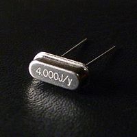
Crystal oscillators are oscillators where the primary frequency determining element is a quartz crystal. Because of the inherent characteristics of the quartz crystal the crystal oscillator may be held to extreme accuracy of frequency stability. Crystal oscillators are usually, fixed frequency oscillators where stability and accuracy are the primary considerations.Temperature compensation may be applied to crystal oscillators to improve thermal stability of the crystal oscillator.
Now most of oscillator using PLL system because it can work with variable frequency, but still using Crystal oscillator as referency that making PLL stable.

This is a typical example of the type of crystal oscillators which may be used for say converters. Some points of interest on crystal oscillators in relation to figure 1.


The transistor could be a general purpose type with an Ft of at least 150 Mhz for HF use. A typical example would be a 2N2222A.

The turns ratio on the tuned circuit depicts an anticipated nominal load of 50 ohms. This allows a theoretical 2K5 ohms on the collector. If it is followed by a buffer amplifier (highly recommended) I would simply maintain the typical 7:1 turns ratio. I have included a formula for determining L and C in the tuned circuits of crystal oscillators in case you have forgotten earlier tutorials. Personally I would make L a reactance of around 250 ohms. In this case I'd make C a smaller trimmer in parallel with a standard fixed value.


edited from : epanorama.net & electronics-tutorial.com

Tuesday, May 8, 2007

Additional LED STOP LAMP

Need More STOP LAMP, using LED?? why not, with the same brightness with Bulb but smaller in power consumption , check this circuit :


Edited from : National T Bucket Association

Emergency Lamp

in my place, blackout lamp is always happend, evenly in night, Fortunately I have Used Car Battrey12 volt, so i'll try to using it to light up my room using little circuit here..


Monday, May 7, 2007

Digital to Analog Converter ( DAC)

make we feel what the computer result, use DAC, to convert digital result data from computer / microcontroller to analog signal (ie. voltage,sound,light), I choose DAC 0830 because its reliable & cheaper :

The DAC0830 is an advanced CMOS/Si-Cr 8-bit multiplying
DAC designed to interface directly with the 8080, 8048,
8085, Z80®, and other popular microprocessors. A deposited
silicon-chromium R-2R resistor ladder network divides the
reference current and provides the circuit with excellent temperature
tracking characteristics (0.05% of Full Scale Range
maximum linearity error over temperature). The circuit uses
CMOS current switches and control logic to achieve low
power consumption and low output leakage current errors.
Special circuitry provides TTL logic input voltage level compatibility.
Double buffering allows these DACs to output a voltage corresponding
to one digital word while holding the next digital
word. This permits the simultaneous updating of any number
of DACs.
The DAC0830 series are the 8-bit members of a family of
microprocessor-compatible DACs (MICRO-DAC™)


and below the sample circuit for audio controlling :

Analog to Digital Converter ( ADC )

Why we need ADC ?

Normally analogue-to-digital con-verter (ADC) needs interfacing through a microprocessor to convert analogue data into digital format. This requires hardware and necessary software, resulting in increased complexity and hence the total cost.


The circuit of A-to-D converter shown here is configured around ADC 0808, avoiding the use of a microprocessor. The ADC 0808 is an 8-bit A-to-D converter, having data lines D0-D7. It works on the principle of successive approximation. It has a total of eight analogue input channels, out of which any one can be selected using address lines A, B and C. Here, in this case, input channel IN0 is selected by grounding A, B and C address lines.
Usually the control signals EOC (end of conversion), SC (start conversion), ALE (address latch enable) and OE (output enable) are interfaced by means of a microprocessor. However, the circuit shown here is built to operate in its continuous mode without using any microprocessor. Therefore the input control signals ALE and OE, being active-high, are tied to Vcc (+5 volts). The input control signal SC, being active-low, initiates start of conversion at falling edge of the pulse, whereas the output signal EOC becomes high after completion of digitisation. This EOC output is coupled to SC input, where falling edge of EOC output acts as SC input to direct the ADC to start the conversion.
As the conversion starts, EOC signal goes high. At next clock pulse EOC output again goes low, and hence SC is enabled to start the next conversion. Thus, it provides continuous 8-bit digital output corresponding to instantaneous value of analogue input. The maximum level of analogue input voltage should be appropriately scaled down below positive reference (+5V) level.
The ADC 0808 IC requires clock signal of typically 550 kHz, which can be easily derived from an astable multivibrator constructed using 7404 inverter gates. In order to visualise the digital output, the row of eight LEDs (LED1 through LED8) have been used, wherein each LED is connected to respective data lines D0 through D7. Since ADC works in the continuous mode, it displays digital output as soon as analogue input is applied. The decimal equivalent digital output value D for a given analogue input voltage Vin can be calculated from the relationship

Saturday, May 5, 2007

Simple 5V & 12V Adapter

Here i give the simple circuit to generate very stable 5VCD and 12VCD :

A basic circuit of the 89C2051

A basic circuit of the 89C2051 shown here can be made easily using point-to-point soldering with a universal PCB. Use an ordinary 20-pin socket, do not use a circle-pin socket. D1 is a small dot LED. U2 can be either 7805 or 78L05. U3 is optional for correcting any polarity DC adapter. Without the 2051 chip in the socket, checks the connection, then measures +5V between pin 20 and pin 10. Test the LED by shorting P1.7 pin to GND.

Test your board with myfirst.c, a simple c program that makes LED blink every 0.5 second.

/*
* myfirst.c
* First C program for 2051 experiment
* complement P1.7 every 0.5 sec
* Copyright (C) 1999 Wichit Sirichote
* compiled with Dunfield Micro-C for 8051 Release 3.2
*/

#include c:\mc\8051io.h /* include i/o header file */
#include c:\mc\8051reg.h

extern register char cputick; // cputick was incremented every 10ms
register unsigned char sec100,flag1;

#define n 50

task1(); // functions declarations
task2();

main()
{
flag1 = 0;
sec100 = 0;
serinit(9600); // set timer0 to be 16 bit counter
while(1){

while(cputick == 0)
;
cputick = 0;
task1();
task2();
}
}

task1() // set bit 0 of flag1 every n*10ms
{
sec100++; // increment sec100
if (sec100 >= n)
{sec100 = 0; // clear sec100
flag1 |= 0x01; // set bit 0 of flag1
}
}

task2()
{
if ((flag1 & 0x01) != 0) // execute below if bit 0 of flag1 is set
{
// P1 ^= 0x80; // exclusive or the latch bit 7 with 0x80
asm " CPL P1.7"; // complement P1.7
flag1 &= ~0x01; // clear bit 0 of flag1
}
}


MYFIRSTC.HEX


Wichit Sirichote, kswichit@kmitl.ac.th

Make Your Own Single-Side PCB for Easy-Downloader V1.1


The Easy Downloader V 1.1 , a Flash Writer for 89C2051/4051 which was designed by Wichit Sirichote, used a Double-Side PCB. I think, it's difficult to make my own PCB by myself. So that I decided to design a Single-Side PCB instead. My first prototype board was made using hand-writing with a permanent ink pen( see later in Figure 3). This page however, thus provides a PCB layout and components placement written by Paint Program. So simple, but it works fine. Everyone can make it easily. If you've got problem or any suggestion, please send it to my e-mail address shown above.
Figure 1: Bottom View of PCB Pattern for Easy Downloader V 1.1 (A full size copy is 6.5x13 cm)

Figure 2: Component placement layout (top view), be careful pin 1 of IC chips and polarity of electrolytic capacitors.

Don't forget, you must connect jumper wires on a bottom of PCB: pin 12-19 of the writer(89c2051) to pin 12-19 of the ZIF Socket, respectively

Figure 3: Shows jumper wires connection on the bottom side of PCB, see the handcraft PCB pattern, so cool !
Single-side PROTEL PCB file, EZSS.PCB

As reference, this is the schematic diagram

1. Blue pattern is copper trace layer on a bottom of the PCB.
2. Yellow pattern is a component overlay.
3. Green lines are jumper lines (J3-J10) which must be connected on the bottom of the PCB.

Source from : Plermjai Inchuay, plermjai@loxinfo.co.th